Design of Frequency Characteristic Tester Based on DSP
Based on the idea of ​​direct digital frequency synthesis technology, a low-cost, digital, and intelligent frequency characteristic tester was designed using modern digital signal processing and display technology. The amplitude and frequency characteristics of the network under test in any frequency band from 20 Hz to 150 MHz are measured. Completed data storage, 3-band bandwidth calculation, peak search and other functions, amplitude detection accuracy of 1dBm, phase detection accuracy of 1 ° and other indicators.
The signal source of the traditional frequency sweeper mostly adopts an oscillator composed of an LC circuit, a large number of discrete components are used to realize each function, and the display part adopts a conventional scanning display. Therefore, the traditional structure of the frequency scan meter is not only complex in structure, large in size, expensive, and complicated in operation. Moreover, due to the large dispersibility of various components, the parameter changes are easily affected by changes in the external environment, and the accuracy is not high. At present, instrument manufacturers represented by Agilent etc. provide a variety of high-performance frequency characteristic testers. However, its products are mainly concentrated in high-frequency fields such as radio frequency and microwave, and products in the low- and mid-frequency bands are relatively scarce. Based on the technical idea of ​​direct digital frequency synthesis (DDS), this paper adopts modern digital signal processing technology based on DSP and FPGA architecture to design a low-cost, highly-digitalized and intelligent frequency characteristic tester, achieving a range of 20Hz to 150MHz. Measurement and display of the amplitude and frequency characteristics of the measured network within any frequency band, complete the data storage and playback, -3dB bandwidth calculation, peak search and other functions. The amplitude detection accuracy reaches 1dBm, and the phase detection accuracy is 1°.
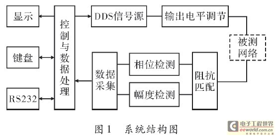
1 system composition frequency characteristic analyzer mainly includes control and data storage processing unit, DDS signal source unit, amplitude and phase detection unit, data acquisition unit, display and interactive interface unit, the overall system block diagram shown in Figure 1.
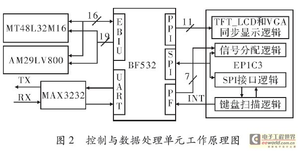
2 system design 2.1 control and data processing unit ADSP-BF532 and FPGA (EP1C3) is the core of the control and data storage processing unit. The DSP performs two-way data communication with the FPGA through the PPI, SPI, and PF interfaces to implement functions such as keyboard reading, DDS scanning, A/D acquisition, and LCD scanning, and realizes data transmission and remote control through the UART unit and the computer. FPGA completed the TFT_LCD and VGA synchronous display timing conversion, keyboard scan, SPI communication and signal distribution functions. In addition, the DSP connects the AM29LV800 and MT48L32M16 as program and working status memories and data storage and display buffers via EBIU units. The working principle is shown in Figure 2.
2.2 Data Acquisition Unit The data acquisition unit uses multiple A/D converters to convert the amplitude and phase analog voltage signals into digital signals for DSP and FPGA processing and transmission. It is a "bridge" between analog and digital circuits. . The instrument uses the AD7655 acquisition signal. The A/D converter has 4 analog input channels, 16-bit sampling accuracy, and a maximum sampling rate of 1 MHz. Uses 16-bit parallel and SPI transmission modes. The REF3125 provides the 2.5V reference voltage required by the A/D converter.
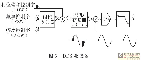
2.3 DDS signal source unit The DDS technology is a synthesis technique that converts a series of digital form signals into analog signals through DACs. DDS technology is based on the sampling theorem. It first samples the waveform to be generated, digitizes the sampled value and stores it into memory as a lookup table. Then the data is read out through a lookup table and converted by a D/A converter. As an analog quantity, the stored waveforms are recombined. Although there are many kinds of structure of DDS system, but its basic circuit principle, as shown in Fig. 3.
The DDS chip AD9958 used in this instrument is a high performance dual-channel direct digital frequency synthesizer with two independent DDS cores with two independent 32-bit frequency control words and 14-bit phase control words, one 10-bit Amplitude control word. Internally integrated PLL, the chip's maximum operating frequency is 500MHz, and the maximum frequency of the output signal can reach 180MHz. DSP through the SPI and PF interface through the FPGA signal distribution logic for the AD9958 frequency, phase and amplitude control word configuration, as shown in Figure 4.

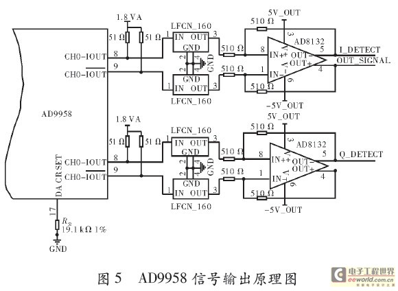
The AD9958 uses a 25-MHz external clock input and generates a 500-MHz core operating clock after being multiplied by the internal PLL. The output signal is two sine and cosine signals of the same frequency. To prevent digital noise from interfering with the signal, the 3.3V digital power supply and the analog power supply of the chip must be isolated using a type of network, and the analog ground is connected to the ground plane to isolate interference. Since the chip output is a current signal, a 51Ω pull-up to 1.8V conversion to a voltage signal is required. The LFCN-160 integrated filter is used to filter out high-frequency noise, and the differential op amp AD8312 is used to cancel the common-mode noise. The output signal level range is -10 ~ -3dBm. AD9958 signal output principle shown in Figure 5.
2.4 Output Level Adjustment Unit The output level of the signal source designed by this instrument ranges from -87 to 13dBm. The level of the output signal of the preceding DDS signal source unit is in the range of -10 to -3 dBm, so it is necessary to adjust the level of the preceding signal. The signal flow diagram of this unit is shown in Figure 6.
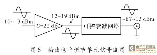
The unit first amplified the pre-signal level to 12-19 dBm through the wideband op amp THS3201. Then, the signal in the range of -87 to 13 dBm is output through a controllable attenuation network. This is achieved by controlling the switching on of different types of resistive decay networks, as shown in Figure 5. The controllable attenuation network consists of four types of resistive attenuation networks: -8dB, -16dB, -32dB, and -64dB. The 68095-driven relay TQ2 combines attenuation networks with different attenuation factors.
2.5 Phase Detection Unit The instrument uses the AD8302 to build a phase difference detection circuit. The AD8302 can accurately measure the amplitude ratio and phase difference between two input signals in the range of 0 to 2.7 GHz and -60 to 0 dBm, with phase detection accuracy of up to 1°. The AD8302 phase detection curve is shown in Figure 7.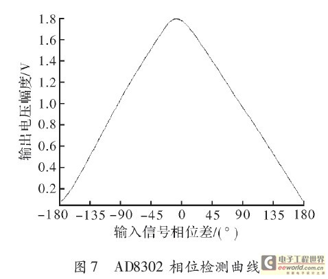
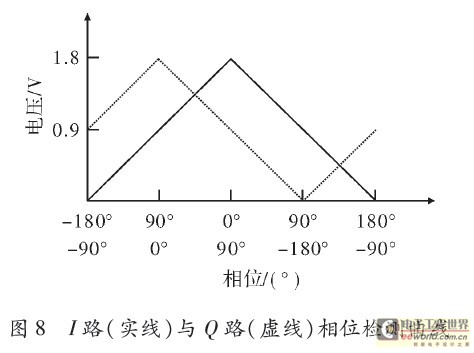
As can be seen from FIG. 7 , the monophase AD8032 cannot perform phase monitoring within the range of −180° to 180°. In order to realize -180°~180° monitor phase, the instrument uses I, Q orthogonal detection method. That is, the DDS signal source outputs two orthogonal signals of the same frequency. The orthogonal signals respectively enter the two AD8302 supervising phases through the two 8302 and the signal to be measured, and then two phase differences can be obtained as 90° phase curves, as shown in FIG. 8 . As shown. This achieves a detection range of -180° to 180°.
2.6 amplitude detection unit The instrument amplitude detection circuit consists of a logarithmic amplifier AD8310 and filter capacitor unit. The AD8310 can detect the amplitude of signals from 0 to 440 MHz and -91 to +4 dBV. The output formula is

Among them, VOUT is the detection output; VY is the slope voltage; VIN is the input signal voltage; VX is the cut-off voltage.
The capacitance of the OFLT and BFIN pins of the AD8310 needs to be adjusted in real time based on the frequency of the sweep. After repeated tests, accurate detection in the range of 20 Hz to 150 MHz can be achieved using a combination of 0.01 μF, 0.1 μF, 1 μF, 10 μF, and 100 μF.
3 Measurement Results This test measures the LPF-BOR8 low-pass filter. The cutoff frequency of this filter is 1.2MHz. After the instrument is powered on, the output level is first set to 0 dBm, the initial frequency is set to 20 Hz, and the termination frequency is set to 1.5 MHz. The output and input of the instrument are then shorted for amplitude and phase correction. After calibration, the output of the instrument is connected to the input of the filter and the output of the filter is connected to the input of the instrument for measurement. The measurement result is shown in Figure 9. As can be seen from the figure, the passband of the filter is relatively stable, the phase tends to be linear, and the -1dB turning point is approximately 1.2MHz, which is in agreement with the data given in the data sheet of the device.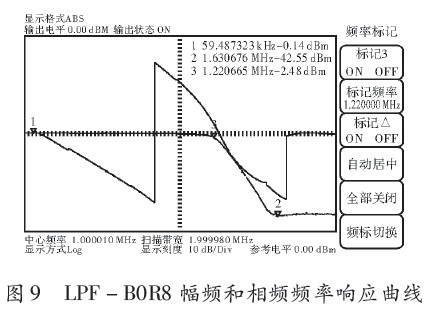
4 Concluding remarks The instrument realizes the measurement of amplitude and phase frequency characteristics, data storage, playback, peak search, -3dB measurement, and Q value search of the measured network in any frequency band from 20 Hz to 150 MHz. Because a large number of large-scale integrated circuits are used, not only the integration of the system is increased, but also the volume is reduced, and the performance and stability of the instrument are improved. Digitalization, intelligence, and low cost have been achieved. At present, the instrument has entered the production stage.
The signal source of the traditional frequency sweeper mostly adopts an oscillator composed of an LC circuit, a large number of discrete components are used to realize each function, and the display part adopts a conventional scanning display. Therefore, the traditional structure of the frequency scan meter is not only complex in structure, large in size, expensive, and complicated in operation. Moreover, due to the large dispersibility of various components, the parameter changes are easily affected by changes in the external environment, and the accuracy is not high. At present, instrument manufacturers represented by Agilent etc. provide a variety of high-performance frequency characteristic testers. However, its products are mainly concentrated in high-frequency fields such as radio frequency and microwave, and products in the low- and mid-frequency bands are relatively scarce. Based on the technical idea of ​​direct digital frequency synthesis (DDS), this paper adopts modern digital signal processing technology based on DSP and FPGA architecture to design a low-cost, highly-digitalized and intelligent frequency characteristic tester, achieving a range of 20Hz to 150MHz. Measurement and display of the amplitude and frequency characteristics of the measured network within any frequency band, complete the data storage and playback, -3dB bandwidth calculation, peak search and other functions. The amplitude detection accuracy reaches 1dBm, and the phase detection accuracy is 1°.
1 system composition frequency characteristic analyzer mainly includes control and data storage processing unit, DDS signal source unit, amplitude and phase detection unit, data acquisition unit, display and interactive interface unit, the overall system block diagram shown in Figure 1.

2 system design 2.1 control and data processing unit ADSP-BF532 and FPGA (EP1C3) is the core of the control and data storage processing unit. The DSP performs two-way data communication with the FPGA through the PPI, SPI, and PF interfaces to implement functions such as keyboard reading, DDS scanning, A/D acquisition, and LCD scanning, and realizes data transmission and remote control through the UART unit and the computer. FPGA completed the TFT_LCD and VGA synchronous display timing conversion, keyboard scan, SPI communication and signal distribution functions. In addition, the DSP connects the AM29LV800 and MT48L32M16 as program and working status memories and data storage and display buffers via EBIU units. The working principle is shown in Figure 2.

2.2 Data Acquisition Unit The data acquisition unit uses multiple A/D converters to convert the amplitude and phase analog voltage signals into digital signals for DSP and FPGA processing and transmission. It is a "bridge" between analog and digital circuits. . The instrument uses the AD7655 acquisition signal. The A/D converter has 4 analog input channels, 16-bit sampling accuracy, and a maximum sampling rate of 1 MHz. Uses 16-bit parallel and SPI transmission modes. The REF3125 provides the 2.5V reference voltage required by the A/D converter.
2.3 DDS signal source unit The DDS technology is a synthesis technique that converts a series of digital form signals into analog signals through DACs. DDS technology is based on the sampling theorem. It first samples the waveform to be generated, digitizes the sampled value and stores it into memory as a lookup table. Then the data is read out through a lookup table and converted by a D/A converter. As an analog quantity, the stored waveforms are recombined. Although there are many kinds of structure of DDS system, but its basic circuit principle, as shown in Fig. 3.

The DDS chip AD9958 used in this instrument is a high performance dual-channel direct digital frequency synthesizer with two independent DDS cores with two independent 32-bit frequency control words and 14-bit phase control words, one 10-bit Amplitude control word. Internally integrated PLL, the chip's maximum operating frequency is 500MHz, and the maximum frequency of the output signal can reach 180MHz. DSP through the SPI and PF interface through the FPGA signal distribution logic for the AD9958 frequency, phase and amplitude control word configuration, as shown in Figure 4.

The AD9958 uses a 25-MHz external clock input and generates a 500-MHz core operating clock after being multiplied by the internal PLL. The output signal is two sine and cosine signals of the same frequency. To prevent digital noise from interfering with the signal, the 3.3V digital power supply and the analog power supply of the chip must be isolated using a type of network, and the analog ground is connected to the ground plane to isolate interference. Since the chip output is a current signal, a 51Ω pull-up to 1.8V conversion to a voltage signal is required. The LFCN-160 integrated filter is used to filter out high-frequency noise, and the differential op amp AD8312 is used to cancel the common-mode noise. The output signal level range is -10 ~ -3dBm. AD9958 signal output principle shown in Figure 5.

2.4 Output Level Adjustment Unit The output level of the signal source designed by this instrument ranges from -87 to 13dBm. The level of the output signal of the preceding DDS signal source unit is in the range of -10 to -3 dBm, so it is necessary to adjust the level of the preceding signal. The signal flow diagram of this unit is shown in Figure 6.

The unit first amplified the pre-signal level to 12-19 dBm through the wideband op amp THS3201. Then, the signal in the range of -87 to 13 dBm is output through a controllable attenuation network. This is achieved by controlling the switching on of different types of resistive decay networks, as shown in Figure 5. The controllable attenuation network consists of four types of resistive attenuation networks: -8dB, -16dB, -32dB, and -64dB. The 68095-driven relay TQ2 combines attenuation networks with different attenuation factors.
2.5 Phase Detection Unit The instrument uses the AD8302 to build a phase difference detection circuit. The AD8302 can accurately measure the amplitude ratio and phase difference between two input signals in the range of 0 to 2.7 GHz and -60 to 0 dBm, with phase detection accuracy of up to 1°. The AD8302 phase detection curve is shown in Figure 7.

As can be seen from FIG. 7 , the monophase AD8032 cannot perform phase monitoring within the range of −180° to 180°. In order to realize -180°~180° monitor phase, the instrument uses I, Q orthogonal detection method. That is, the DDS signal source outputs two orthogonal signals of the same frequency. The orthogonal signals respectively enter the two AD8302 supervising phases through the two 8302 and the signal to be measured, and then two phase differences can be obtained as 90° phase curves, as shown in FIG. 8 . As shown. This achieves a detection range of -180° to 180°.

2.6 amplitude detection unit The instrument amplitude detection circuit consists of a logarithmic amplifier AD8310 and filter capacitor unit. The AD8310 can detect the amplitude of signals from 0 to 440 MHz and -91 to +4 dBV. The output formula is
Among them, VOUT is the detection output; VY is the slope voltage; VIN is the input signal voltage; VX is the cut-off voltage.
The capacitance of the OFLT and BFIN pins of the AD8310 needs to be adjusted in real time based on the frequency of the sweep. After repeated tests, accurate detection in the range of 20 Hz to 150 MHz can be achieved using a combination of 0.01 μF, 0.1 μF, 1 μF, 10 μF, and 100 μF.
3 Measurement Results This test measures the LPF-BOR8 low-pass filter. The cutoff frequency of this filter is 1.2MHz. After the instrument is powered on, the output level is first set to 0 dBm, the initial frequency is set to 20 Hz, and the termination frequency is set to 1.5 MHz. The output and input of the instrument are then shorted for amplitude and phase correction. After calibration, the output of the instrument is connected to the input of the filter and the output of the filter is connected to the input of the instrument for measurement. The measurement result is shown in Figure 9. As can be seen from the figure, the passband of the filter is relatively stable, the phase tends to be linear, and the -1dB turning point is approximately 1.2MHz, which is in agreement with the data given in the data sheet of the device.

4 Concluding remarks The instrument realizes the measurement of amplitude and phase frequency characteristics, data storage, playback, peak search, -3dB measurement, and Q value search of the measured network in any frequency band from 20 Hz to 150 MHz. Because a large number of large-scale integrated circuits are used, not only the integration of the system is increased, but also the volume is reduced, and the performance and stability of the instrument are improved. Digitalization, intelligence, and low cost have been achieved. At present, the instrument has entered the production stage.
Tactical Gun Slings,Sling With Metal Hook,Gun Slings Rifle Tactical,Outdoor Tactical Hunting Accessories
Guangzhou Miaozhun Jie Trade Co.,Ltd. , https://www.focuhunter.shop
